1 上海大学 微电子学院, 上海 201800
2 上海微技术工业研究院, 上海 201800
3 中国科学院上海微系统与信息技术研究所, 上海 200050
在新型掺钪(Sc)氮化铝(Al1-xScxN)集成光学平台上设计了插入损耗低、传输通道谱线平坦的O波段四通道波分(解)复用器, 并提出了优化方法。所设计的器件结构基于级联马赫-曾德尔干涉仪(MZI)滤波器, 结合弯曲波导结构的定向耦合器改善波长敏感度。针对粗波分复用(CWDM)应用的特性, 文章使用粒子群算法(PSO)提升器件性能优化的效率, 通过调整器件结构的设计参数对四路通道的传输谱线质量进行优化。针对0%, 9%, 23%的掺Sc浓度, 设计的解复用器表现出宽达约15.6nm的1-dB带宽和小于0.1dB的插入损耗, 传输谱线呈“盒状”响应, 各通道间串扰均优于-30.6dB。
硅光子学 波分复用 马赫-曾德尔干涉仪 掺钪氮化铝 silicon photonics WDM MZI scandium-doped aluminum nitride
超构表面是由亚波长结构单元组成,它可以利用微纳制造工艺在平面上制造出来。通过改变超构单元的形貌以及排列方式可以实现对光的精确控制,从而使超构表面实现多种光学器件的功能。超构表面平面光学器件具有超薄、超轻、可芯片级集成、易于大规模量产等优点,近些年来成为了微纳光子学里最热门的研究领域之一。基于紫外光刻工艺的晶圆级加工技术是未来实现超构表面光学器件大规模量产最可行的路线之一。本文综述了近些年来基于紫外光刻技术的晶圆级超构表面光学所取得的进展。这些研究工作在不同尺寸和材料的晶圆上实现了超透镜、偏振带通滤波器、半波片、完美吸收体、光束偏转器等光学器件。
超构表面 光学 CMOS 纳米光子学 晶圆加工 Metasurface Optics CMOS Nanophotonics Wafer processing 光子学报
2021, 50(10): 1024002
Author Affiliations
Abstract
1 Institute of Microelectronics, A*STAR (Agency for Science, Technology and Research), Singapore 138634, Singapore
2 Current Address: School of Microelectronics Science and Technology, Sun Yat-sen University, Zhuhai 519082, China
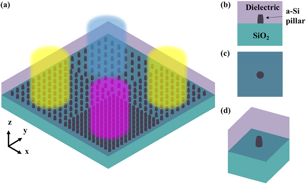
Optical color filters are widely applied in many areas including display, imaging, sensing, holography, energy harvest, and measurement. Traditional dye-based color filters have drawbacks such as environmental hazards and instability under high temperature and ultraviolet radiation. With advances in nanotechnology, structural color filters, which are based on the interaction of light with designed nanostructures, are able to overcome the drawbacks. Also, it is possible to fabricate structural color filters using standard complementary metal-oxide-semiconductor (CMOS) fabrication facilities with low cost and high volume. In this work, metasurface-based subtractive color filters (SCFs) are demonstrated on 12-inch (300-mm) glass wafers using a CMOS-compatible fabrication process. In order to make the transmissive-type SCF on a transparent glass wafer, an in-house developed layer transfer process is used to solve the glass wafer handling issue in fabrication tools. Three different heights of embedded silicon nanopillars (110, 170, and 230 nm) are found to support magnetic dipole resonances. With pillar height and pitch variation, SCFs with different displayed colors are achieved. Based on the resonance wavelength, the displayed color of the metasurface is verified within the red-yellow-blue color wheel. The simulation and measurement results are compared and discussed. The work provides an alternative design for high efficiency color filters on a CMOS-compatible platform, and paves the way towards mass-producible large-area metasurfaces.
Photonics Research
2021, 9(1): 01000013


